Basics of ADS Layout: Master Your RF PCB Design! A guide to the rf pcb design
If you are looking for 3 Enhanced Basics of RF/Microwave PCB Design | MV Flex Circuit you've visit to the right web. We have 25 Pictures about 3 Enhanced Basics of RF/Microwave PCB Design | MV Flex Circuit like Rf PCB | FX PCB, Rf Pcb Design Guidelines Outlet Clearance | brunofuga.adv.br and also Basics of RF PCB Design: Key Concepts and Considerations. Read more:
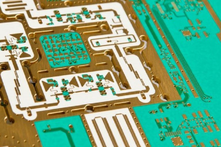
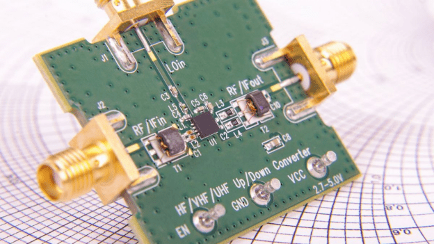
3 Enhanced Basics Of RF/Microwave PCB Design | MV Flex Circuit
 www.flexiblepcbboard.com
3 Enhanced Basics of RF/Microwave PCB Design | MV Flex Circuit
Rf Design Guidelines Pcb Layout And Circuit Optimizat - Vrogue.co
 www.vrogue.co
Rf Design Guidelines Pcb Layout And Circuit Optimizat - vrogue.co
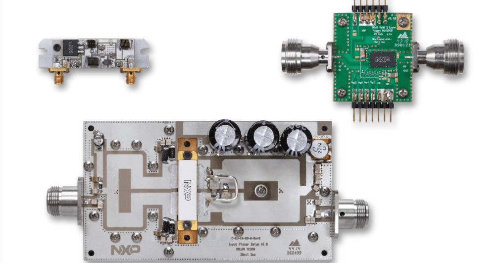
A Guide To The RF PCB Design
 hillmancurtis.com
A Guide to the RF PCB Design
RF PCB Antenna Design | FlowCAD
 www.flowcad.com
RF PCB Antenna Design | FlowCAD
Antenna Design And Rf Layout Guidelines - Design Talk
 design.udlvirtual.edu.pe
Antenna Design And Rf Layout Guidelines - Design Talk
RF PCB Design: A Practical Guide For Engineers | Viasion
 www.viasion.com
RF PCB Design: A Practical Guide for Engineers | Viasion
RF PCB Design | Best Practices For RF Circuit Design, PCB Tips
 www.ourpcb.com
RF PCB Design | Best Practices for RF Circuit Design, PCB Tips
What Are The Types Of RF Filters? - RayPCB
 www.raypcb.com
What are the Types of RF Filters? - RayPCB
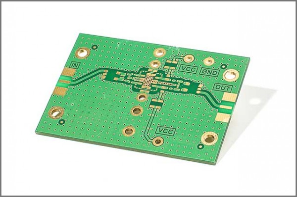
Rf Pcb Layout
 mavink.com
Rf Pcb Layout
How To Create ESP8266 PCB Design - RayMing PCB
 www.raypcb.com
How to Create ESP8266 PCB Design - RayMing PCB
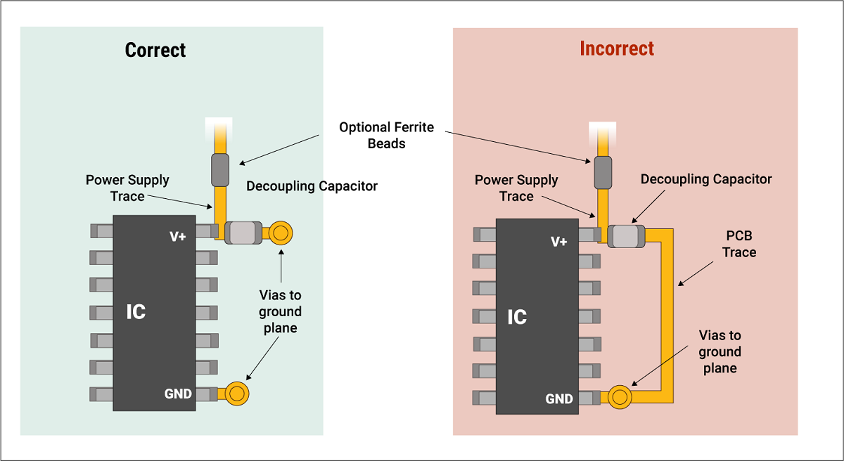
7 Factors That Impact RF PCB Design | Sierra Circuits
 www.protoexpress.com
7 Factors that Impact RF PCB Design | Sierra Circuits
RF PCB Layout Overview - The Engineering Knowledge
 www.theengineeringknowledge.com
RF PCB Layout Overview - The Engineering Knowledge
Basics Of RF PCB Design: Key Concepts And Considerations
 www.viasion.com
Basics of RF PCB Design: Key Concepts and Considerations
The Digital Engineer's Guide To RF PCB Design Guidelines: Layout And R
 www.pcb-hero.com
The Digital Engineer's Guide to RF PCB Design Guidelines: Layout and R ...
RF PCB Design Guidelines From Experienced RF Engineers
 www.viasion.com
RF PCB Design Guidelines From Experienced RF Engineers
Rf Pcb Design Guidelines Outlet Clearance | Brunofuga.adv.br
 brunofuga.adv.br
Rf Pcb Design Guidelines Outlet Clearance | brunofuga.adv.br
Umhlahlandlela Ophelele We-RF PCB Design
 hilelectronic.com
Umhlahlandlela Ophelele we-RF PCB Design
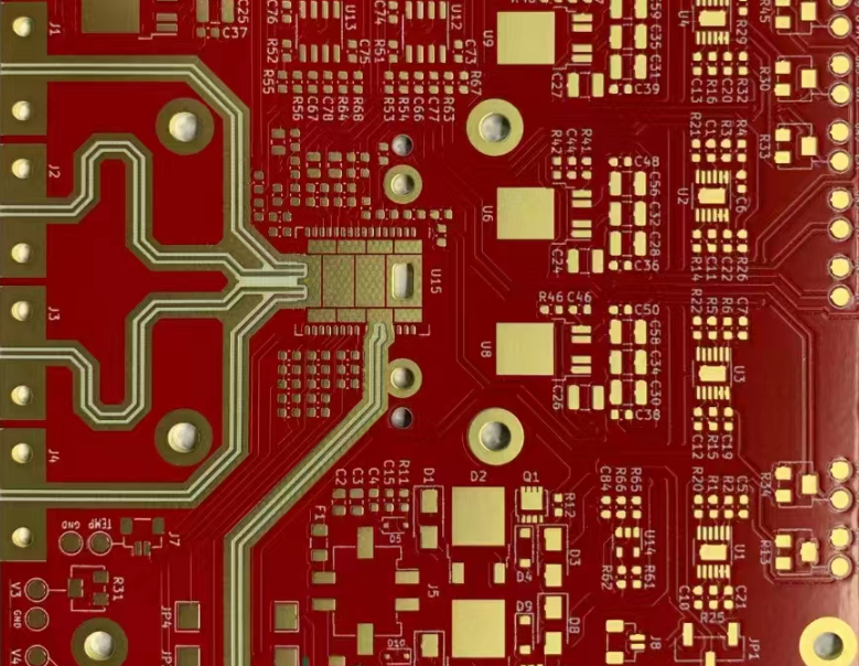
Mastering RF PCB Design And Manufacturing: A Comprehensive Guide
 www.globalwellpcba.com
Mastering RF PCB Design and Manufacturing: A Comprehensive Guide ...
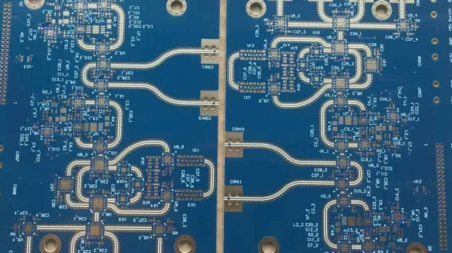
RF PCB Design And Manufacturing
 www.hemeixinpcb.com
RF PCB Design and Manufacturing
RF PCB Design Guidelines You Must Know - RayPCB
 www.raypcb.com
RF PCB Design Guidelines You Must Know - RayPCB
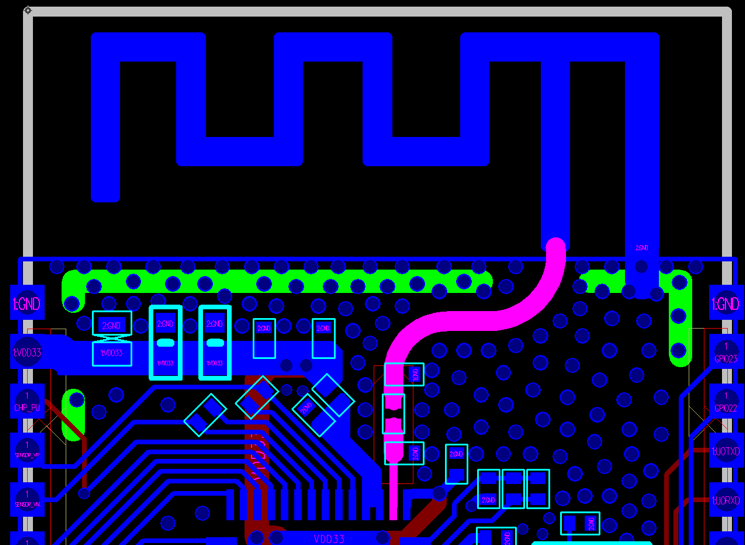
PCB Layout Design - ESP32 - — ESP Hardware Design Guidelines Latest
 docs.espressif.com
PCB Layout Design - ESP32 - — ESP Hardware Design Guidelines latest ...
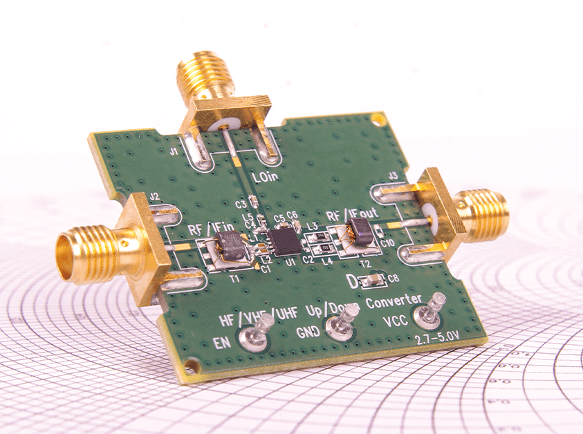
Rf PCB | FX PCB
 sfxpcb.com
Rf PCB | FX PCB
Getting Started With RF PCB Layout Guidelines
 www.hemeixinpcb.com
Getting Started With RF PCB Layout Guidelines
Comprehensive Guide To RF PCB Design
 hilelectronic.com
Comprehensive Guide to RF PCB Design
A Guide To The RF PCB Design
 hillmancurtis.com
A Guide to the RF PCB Design
Rf pcb layout. Rf pcb antenna design. Antenna design and rf layout guidelines