PADS Standard/Plus Viewer: Simplify Your PCB Design Process! pads standard/plus viewer
If you are looking for PCB Design Engineer Resume Sample (2023) you've visit to the right page. We have 25 Pictures about PCB Design Engineer Resume Sample (2023) like The PCB Design Process For Advanced Electronics | Northwest Engineering, PCB Process Flow Chart | www.homillux.com and also PCB Layout Design par Siemens | PADS Professional | Cadlog. Here you go:
PCB Design Engineer Resume Sample (2023)
 itchol.com
PCB Design Engineer Resume Sample (2023)
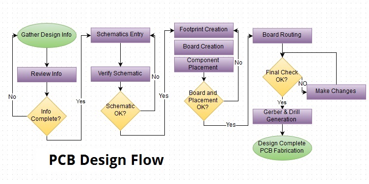
Pcb Design Process Flow At Louise Whipple Blog
 storage.googleapis.com
Pcb Design Process Flow at Louise Whipple blog
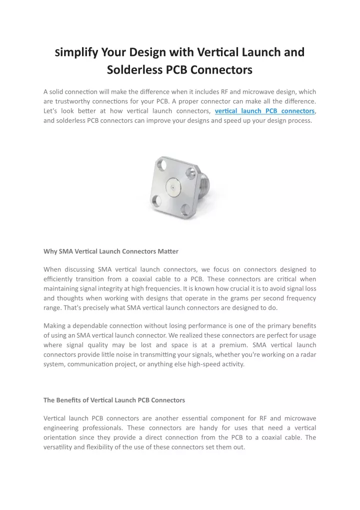
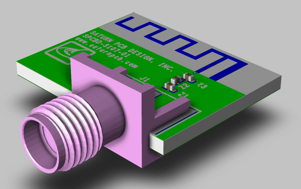
PPT - Simplify Your Design With Vertical Launch And Solderless PCB
 www.slideserve.com
PPT - Simplify Your Design with Vertical Launch and Solderless PCB ...
Baru 10 Pcb Etching Process Simple Dan Minimalis
 skemasupergalaxy.blogspot.com
Baru 10 Pcb Etching Process Simple Dan Minimalis
How To Calculate PCB Design Cost? - RayPCB
 www.raypcb.com
How to calculate PCB design cost? - RayPCB
Basic Steps To Design A PCB Layout – PCB HERO
 www.pcb-hero.com
Basic Steps to Design a PCB Layout – PCB HERO
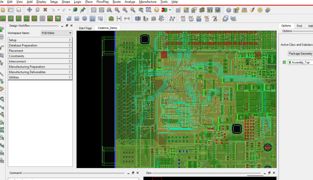
PADS Standard & PADS Standard Plus - PCB Design Software | Siemens Software
 eda.sw.siemens.com
PADS Standard & PADS Standard Plus - PCB Design Software | Siemens Software
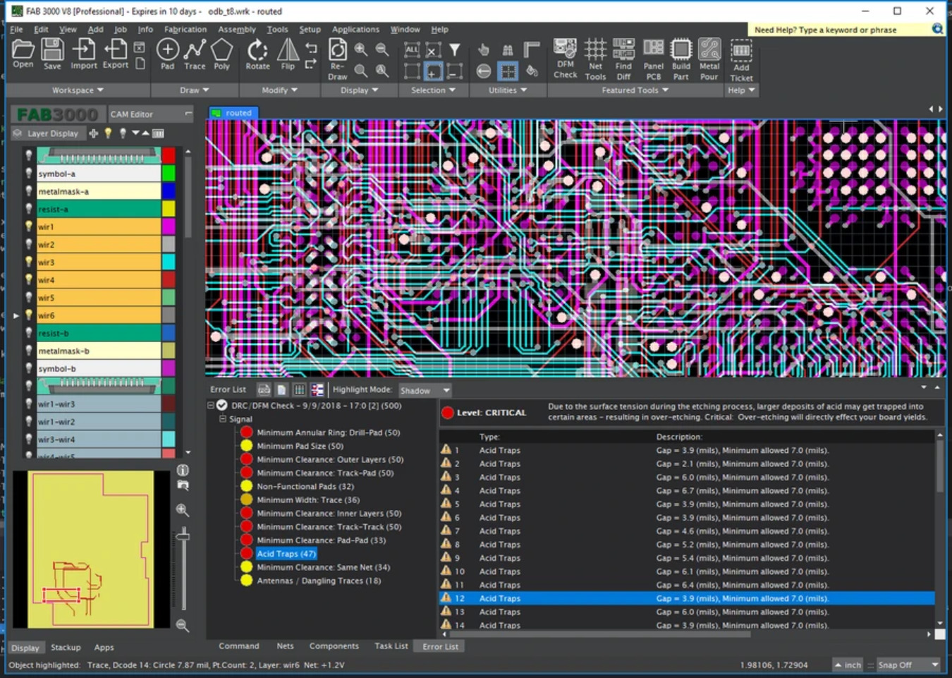
Free Pads Pcb Viewer - Newbuyer
 newbuyer100.weebly.com
Free Pads Pcb Viewer - newbuyer
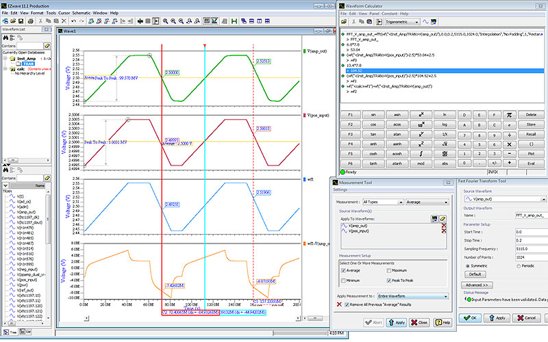
PADS Standard/Plus Viewer | Siemens Software
 resources.sw.siemens.com
PADS Standard/Plus Viewer | Siemens Software
PADS Standard/Plus Viewer | Siemens Software
 resources.sw.siemens.com
PADS Standard/Plus Viewer | Siemens Software
How To Draw PCB And Design PCB Schematics? – PCB HERO
 www.pcb-hero.com
How To Draw PCB and Design PCB Schematics? – PCB HERO
Better Free Allegro Viewer Orcad Lite — RobsPCB PCB, 45% OFF
 www.micoope.com.gt
Better Free Allegro Viewer Orcad Lite — RobsPCB PCB, 45% OFF
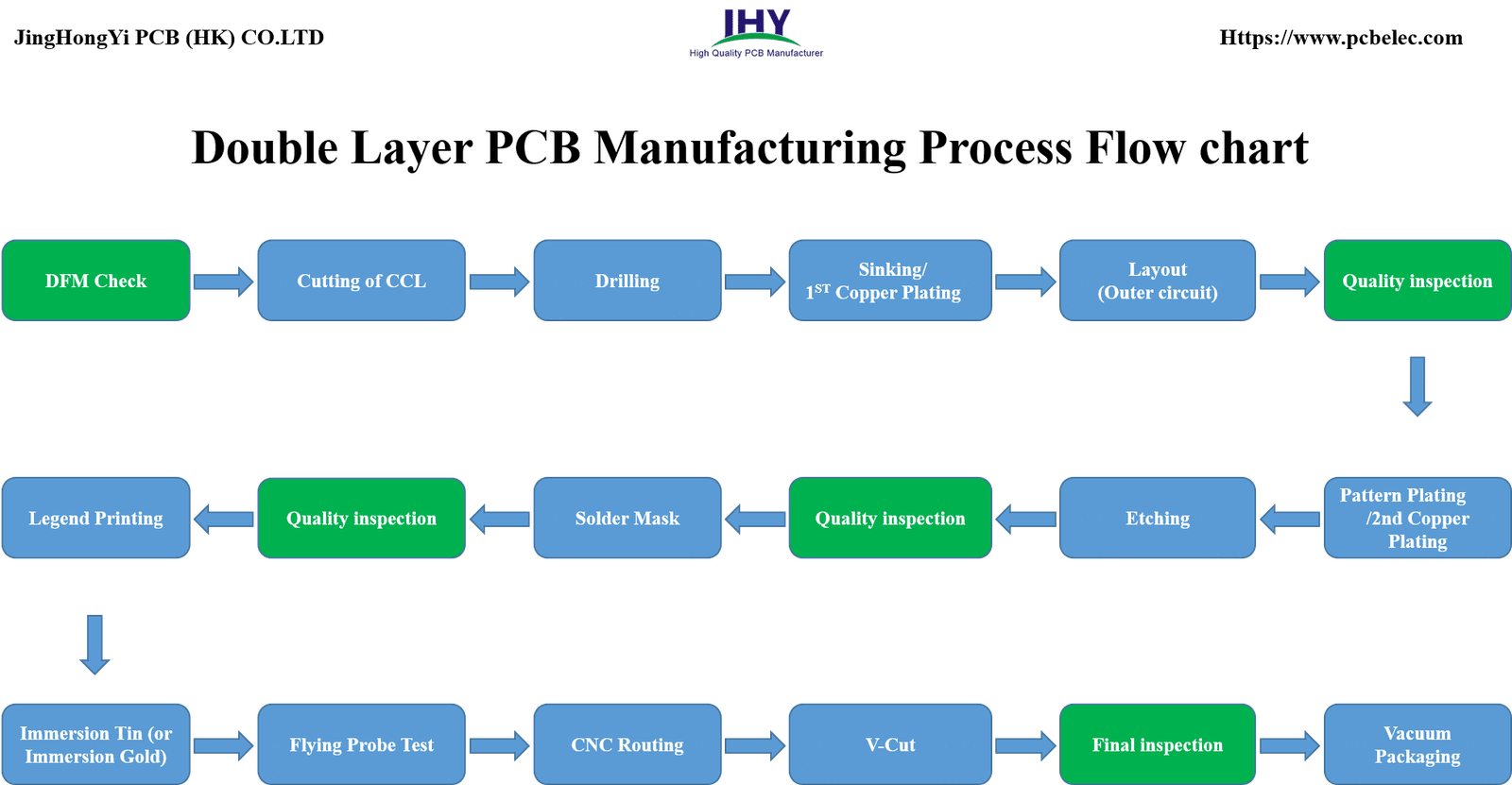
PCB Process Flow Chart | Www.homillux.com
 www.homillux.com
PCB Process Flow Chart | www.homillux.com
The PCB Design Process For Advanced Electronics | Northwest Engineering
 www.nwengineeringllc.com
The PCB Design Process For Advanced Electronics | Northwest Engineering ...
PCB Layout Design Par Siemens | PADS Professional | Cadlog
 www.cadlog.fr
PCB Layout Design par Siemens | PADS Professional | Cadlog
6 Layer Pcb Design Guidelines - Design Talk
 design.udlvirtual.edu.pe
6 Layer Pcb Design Guidelines - Design Talk
How To Design A PCB Antenna?
 www.nextpcb.com
How to Design a PCB Antenna?
Siemens PADS Standard/Plus Viewer - (I)IoT Security News
 iotsecuritynews.com
Siemens PADS Standard/Plus Viewer - (I)IoT Security News
How To Use A Modular Approach To Simplify Your PCB Design Process
 www.linkedin.com
How to Use a Modular Approach to Simplify Your PCB Design Process
Pads Layout Viewer Download: The Key To Streamlining Your PCB Design
 www.raypcb.com
Pads Layout Viewer Download: The Key to Streamlining Your PCB Design ...
PADS Standard/Plus Viewer | Siemens Software
 resources.sw.siemens.com
PADS Standard/Plus Viewer | Siemens Software
Pcb Design Steps - Design Talk
 design.udlvirtual.edu.pe
Pcb Design Steps - Design Talk
Free Pcb File Viewer - Coachingpoo
 coachingpoo.weebly.com
Free pcb file viewer - coachingpoo
PCB Process Flow Chart | Www.homillux.com
 www.homillux.com
PCB Process Flow Chart | www.homillux.com
Pads Layout Viewer Download: The Key To Streamlining Your PCB Design
 www.raypcb.com
Pads Layout Viewer Download: The Key to Streamlining Your PCB Design ...
Pads standard/plus viewer. How to use a modular approach to simplify your pcb design process. Pcb design engineer resume sample (2023)